Title: Meta Devices from Optics to Quantum
Abstract:
Meta-devices enable mass-production of nano-arrays via semiconductor microelectronics, controlling the phase, polarization, and amplitude electromagnetic waves. This talk highlights optical meta-devices’ design, fabrication, and applications in imaging, sensing, 6G, quantum light, and more, unlocking innovations in robotics, AR/VR, healthcare, and quantum technologies.
Specially engineered meta-structure components enable the mass production of artificial nano-array structures using advanced semiconductor microelectronics fabrication techniques. These components possess the capability to manipulate the phase, polarization, and amplitude of electromagnetic waves with exceptional precision. Meta-devices offer solutions to a wide range of pressing technological demands, including novel functionalities, compact size, lightweight design, enhanced efficiency, superior performance, broadband operation, reduced energy consumption, and seamless compatibility with semiconductor mass production technologies. Such attributes position meta-devices as transformative tools for addressing the challenges of next-generation applications.
This work presents a comprehensive overview of the design, fabrication, and emerging applications of optical meta-devices, including achromatic meta-lenses, advanced imaging systems, intelligent sensing plat-forms, vacuum ultraviolet light generation through nonlinear processes, and cutting-edge solutions for medical and biological imaging. Additionally, we highlight their pivotal roles in enabling technologies such as 6G communications, tunable meta-structures, and high-dimensional quantum light sources. These advancements demonstrate the transformative potential of meta-devices in driving the next generation of innovations across diverse fields, including micro-robotic vision, autonomous driving, particle sensing, virtual and augmented reality, personal security systems, biomedical devices, advanced healthcare solutions, and quantum information technologies. By opening new frontiers, optical meta-devices are prepared to redefine technological possibilities and catalyze progress across multiple disciplines.
Biography:
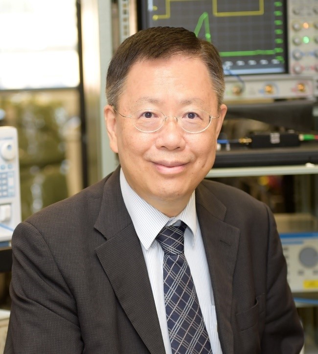
Professor Din-Ping Tsai is currently Chair Professor of the Department of Electrical Engineering, City University of Hong Kong. He is an elected Fellow of AAAS, APS, COS, EMA, IEEE, JSAP, NAI, OSA, SPIE, PST, and AAIA, respectively. He is also an elected Member of the Hong Kong Academy of Engineering (HKAE), International Academy of Engineering (IAE), and Academician of the Asia-Pacific Academy of Materials (APAM), respectively. He is the author and co-author of 410 SCI papers, 70 book chapters and conference papers, and 39 technical reports and articles. He was granted 69 patents for 45 innovations. He was invited as an invited speaker for international conferences or symposiums more than 355 times (31 Plenary Talks, 66 Keynote Talks). He received more than 40 prestigious recognitions and awards, including “Mozi Award” from the International Society of Optical Engineering (SPIE) in 2018; “Global Highly Cited Researchers,” by Web of Science Group (Clarivate Analytics) in 2020 and 2019, respectively; China’s Top 10 Optical Breakthroughs in 2020 and 2018, respectively; 2024 Frontiers of Science Award; etc. He currently serves as a member of the editorial board of 12 prestigious Journals, and Editor of Light: Advanced Manufacturing, and "Photonics Insights," respectively.

Title: 30 years of Nanoimprint: past development and current momentum
Abstract:
2025 marks the 30th anniversary of nanoimprint lithography (NIL). Since its inception in 1995, and through global efforts over the past three decades, Nanoimprint has emerged as the primary alternative to EUV lithography for deep-nanoscale silicon electronics. The manufacturing quality of NIL was recognized by several semiconductor companies and has been actively evaluated for advanced semiconductor devices. Nanoimprinting's potential extends beyond silicon chip fabrication and wafer-scale application—it has demonstrated intriguing capabilities including high resolution, large-scale patterning, 3D capabilities, and low cost of ownership. NIL has also faced challenges such as defect density and quality concerns. Various technologies were developed over time. This talk aims to provide a balanced overview of the pros and cons of NIL, presenting the solutions and advancements that have shaped its progress. We will also describe some of our efforts and results at the University of Michigan that spans over a decade. The application of NIL in industrial manufacturing represents a significant milestone, which include advancements in semiconductor IC circuits, cutting-edge optical devices, and other innovative applications. It is anticipated that even more applications will emerge in the near future.
Biography:
L. Jay Guo is a Professor of Electrical and Computer Engineering at the University of Michigan, where he joined in 1999 after his PhD and postdoc training, and Director of the Macromolecular Science and Engineering at UM. Professor Guo’s lab is involved in interdisciplinary research, with activities ranging from polymer-based photonic devices and sensor applications, flexible transparent conductors, nanophotonics, structural colors and AI assisted design, hybrid photovoltaics and photodetectors, to nanomanufacturing technologies, and are contributed by students from Electrical Engineering and Optics, Macromolecular Science & Engineering, Applied Physics, Physics, and Mechanical Engineering. Prof. Guo has 295 journal publications; with citation more than 34,400 times, and an H-index of 92 (by google scholar). Some notable awards he received from recent years include 2023 Wise-Najafi Prize for Engineering Excellence in the Miniature World from University of Michigan, 2017 William Mong Distinguished Lecturer in Hong Kong University, and 2015 Monroe-Brown Research Excellence Award by the College of Engineering of University of Michigan. He is a fellow of IEEE and a fellow of Optica. His professional service includes Associate Editor of Optica (2018~2021); and currently member of the Editorial Advisory Board of Advanced Optical Materials, and Opto-electric Science, co-Editor-in-Chief of Micro and Nano Manufacturing. His entrepreneur activities include co-founding two startup companies to commercialize technologies from his lab.
Title: Atomaterials for Sustainability
Abstract:
“Atomaterials” represents materials with at least one dimension on the atomic scale. Their properties depend on the precise configuration of their atoms. It is a new but rapidly developing field. A typical atomaterials is graphene, which is made of carbon atoms. Unlike diamond, in which the carbon atoms form a rigid three-dimensional structure, graphene is made of single layer of carbon atoms, bonded together in a two-dimensional honeycomb lattice. They show exceptional properties due to their atomaterials nature. Using atomaterials, our lab has been working on a range of innovations, at various stages of development, for example: A diurnal cooling film without consuming electricity. This film can cool the environment by up to 15°C without using any electricity. By integrating such a film into a building, the electricity used for air conditioning can be dramatically reduced. This will not only save electricity bills but also reduce greenhouse emissions; Heat-absorbing film, achieving over 97% of energy conversion rate with an ultrathin film arrangement. These materials play critical role in improving energy efficiency and providing innovative sustainable solutions for our society.
Biography:
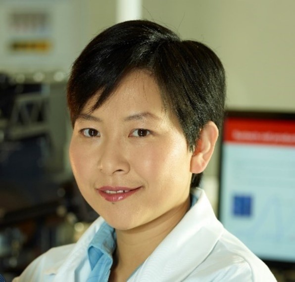
Distinguished Professor Baohua Jia is the inaugural Director of Centre for Atomaterials and Nanomanufacturing (CAN), a Key Chief Investigator (CI) of The Australian Research Council (ARC) Research Hub for Intelligent Energy Efficiency in Future Protected Cropping, a Key CI in ARC Industrial Transformation Training Centre in Surface Engineering for Advanced Materials (SEAM) and Node Director of ARC Centre of Excellence in Optical Microcombs for Breakthrough Science (COMBS). She is an elected Fellow of Australian Academy of Technological Sciences and Engineering (FTSE), and an elected Fellow of OPTICA and Institute of Materials, Minerals and Mining. Her research focuses on the fundamental light and nanomaterial interaction, in particular, laser manipulation of two-dimensional materials for effective harnessing and storage of clean energy from sunlight; purifying water and air for clean environment; imaging and spectroscopy and nanofabrication using ultrafast laser towards fast-speed all-optical communications and intelligent manufacturing.

Title: Materials Solutions for Sustainability Challenges
Abstract:
Micro/nanostructured materials offer significantly new opportunities for high-efficiency devices and systems for energy harvesting, conversion and storage. There is, however, a tremendous gap between the proof-of-principle demonstrations at the small scale and the intrinsically large-scale real-world energy systems and sustainable applications. In this talk, I will give an overview of our research and, more specifically, present our recent development on how structured photonic materials address the challenge of the tremendous power hungry for space cooling, promote photosynthesis and crop yield in greenhouses, and beyond.
Biography:
Dr. Xiaobo Yin received his PhD from Stanford University in 2008 and is currently a Professor of Mechanical Engineering and a Professor of Physics at the University of Hong Kong. He is a fellow of OSA and SPIE. Prior to joining the University of Hong Kong, he was the Bruce S. Anderson Faculty Fellow of the College of Engineering and Applied Sciences at the University of Colorado Boulder. His research focuses on nanostructured optical materials, radiative heat transfer, high-temperature materials, and scalable manufacturing.His works have been featured in numerous media outlets including Nature, Science, Physics Today, Scientific American, the Economists, and Forbes. He was a recipient of the 2017 Moore Inventor Fellowships, the 2017 Kavli Foundation Early Career Lectureship of Materials Science, and the 2022 Xplorer Prize. His work on passive radiative cooling was named one of the top 10 breakthroughs of the year 2017 by the Institute of Physics (IOP) Physics World and the top 10 most reviewed news by The Economists.

Title: Grayscale Laser Beam Lithography for Large Area Surface Engineering: Accelerating the Lab-to-Fab Transition
Abstract:
The rapid industrialization of micro‑ and nano‑optics for consumer electronics demands manufacturing platforms that can reliably deliver complex features—free‑form optical elements, stitch‑free large‑area gratings, deep microlens arrays, and holographic textures—at commercially viable speeds and costs.
Grayscale laser‑beam lithography (GS‑LBL) has evolved over the past four decades into a cornerstone technology for wafer‑scale fabrication. When integrated with multibeam direct‑write exposure, GS‑LBL now emerges as an advanced manufacturing method for patterning surface‑relief profiles on panel‑scale glass substrates while eliminating the need for step‑and‑repeat recombination approaches, which are prone to stitching artifacts. Our latest generation systems pair deep‑sub‑micron level (<600 nm) critical dimension resolution with real-time 8-bit dynamic range grayscale capabilities and aerial throughputs above 500 mm²/min, positioning it both as a competitive stand‑alone solution for low‑ to medium‑volume production and as a master origination tool for downstream processing, such as nano‑imprint replication.
We will highlight recent achievements—including large area diffraction gratings, ultra‑deep microlens arrays, holographic surfaces and diffusers—and present integrated workflows that link LBL to Raith’s complementary direct‑write and metrology platforms.
This closed‑loop ecosystem accelerates design‑to‑prototype iteration, drives process control and metrology capabilities for yield improvement and shortens the lab‑to‑fab transfer cycle, thereby enabling cost‑effective deployment of micro‑/nano‑textured optics across the next‑generation consumer products.
Biography:
Dr. Kahraman Keskinbora is a Netherlands based materials scientist and nanofabrication expert who is the Product Manager for Laser Beam lithography systems at Raith Group. After completing his B.Sc. and M.Sc. degrees in Materials Science and Nanotechnology, at the Andolu University in Türkiye, he earned his Ph.D. degree at the Max Planck Institute for Intelligent Systems and the University of Stuttgart, where he pioneered binary and grayscale ion beam lithography for high efficiency X-ray optics. Later, he led the Micro/Nano-Optics Research Group at MPI-IS, where his group developed the first ever 3 D nanoprinted polymer kinoform lenses for soft X-rays. A former visiting scholar at Harvard University and a DFG-funded Research Scientist at MIT, he has co-authored 40 plus papers, holds multiple patents on micro and nano optics. Dr. Keskinbora frequently presents at optics and nanotechnology conferences, leads professional workshops, and mentors early career researchers, reflecting his commitment to translating nanoscale research into practical photonics and lithography solutions.